Manufacturer & Trading Company
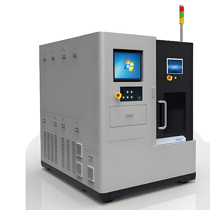
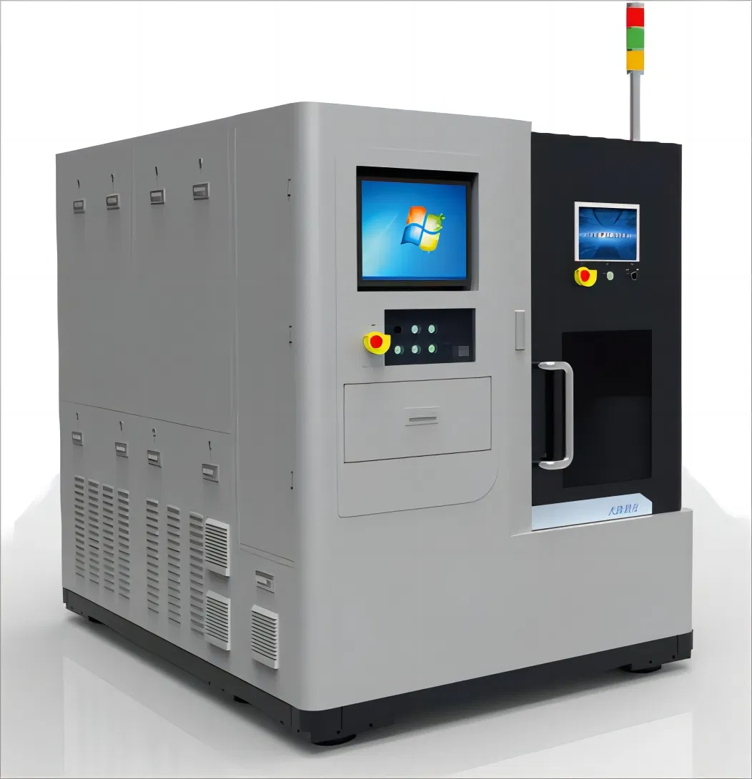
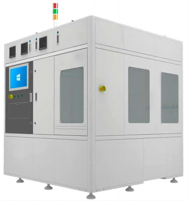
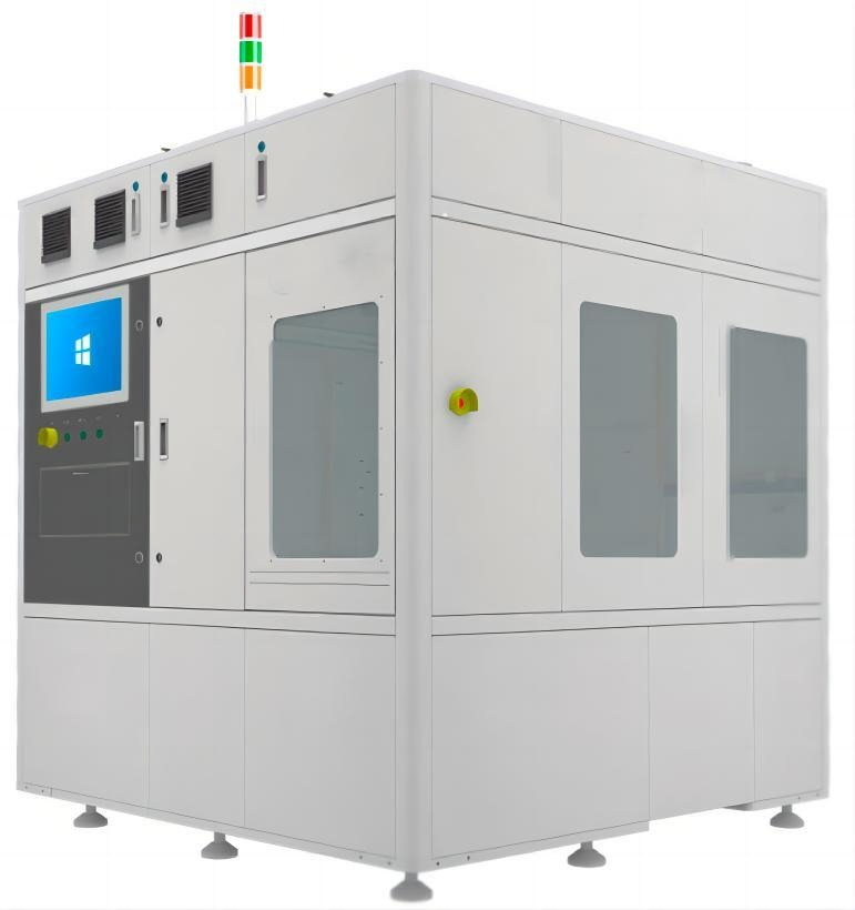
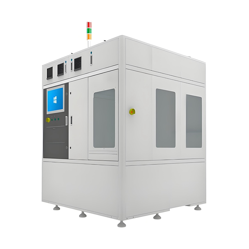
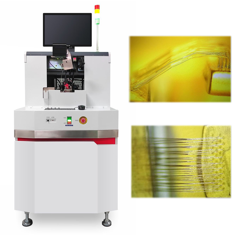
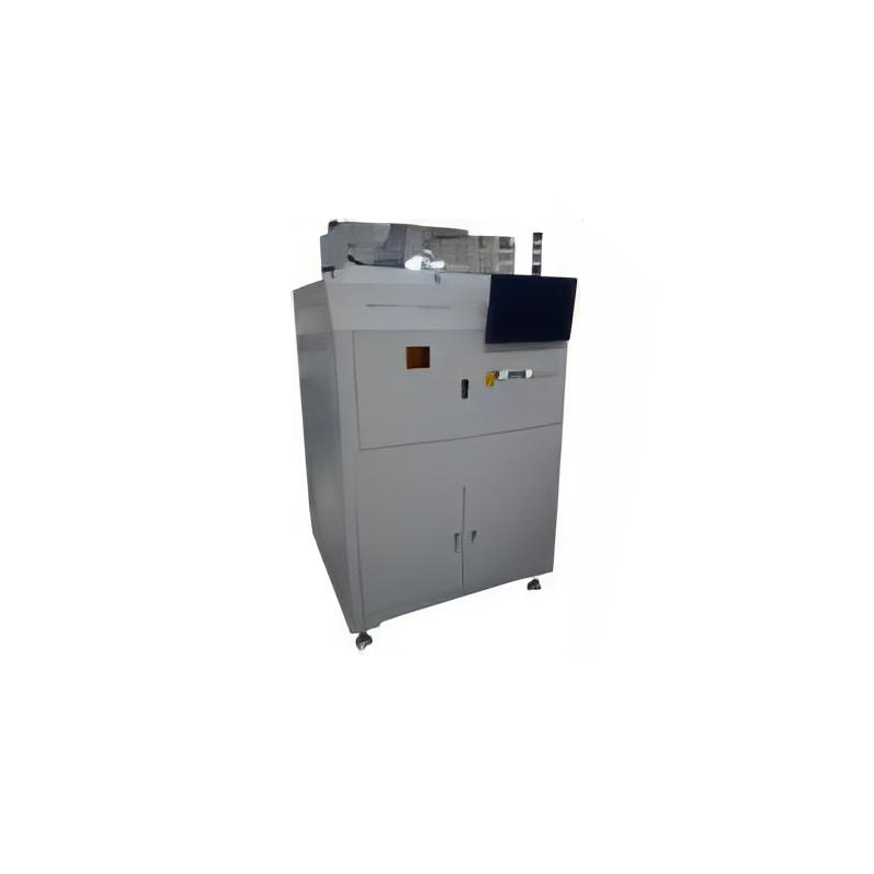
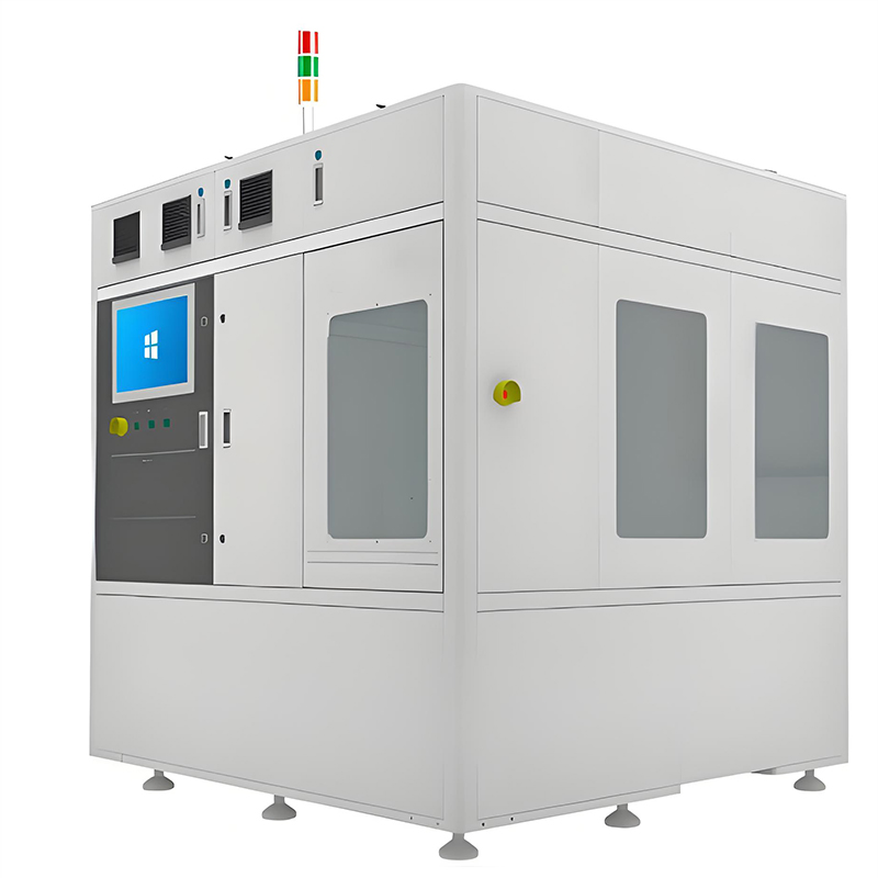
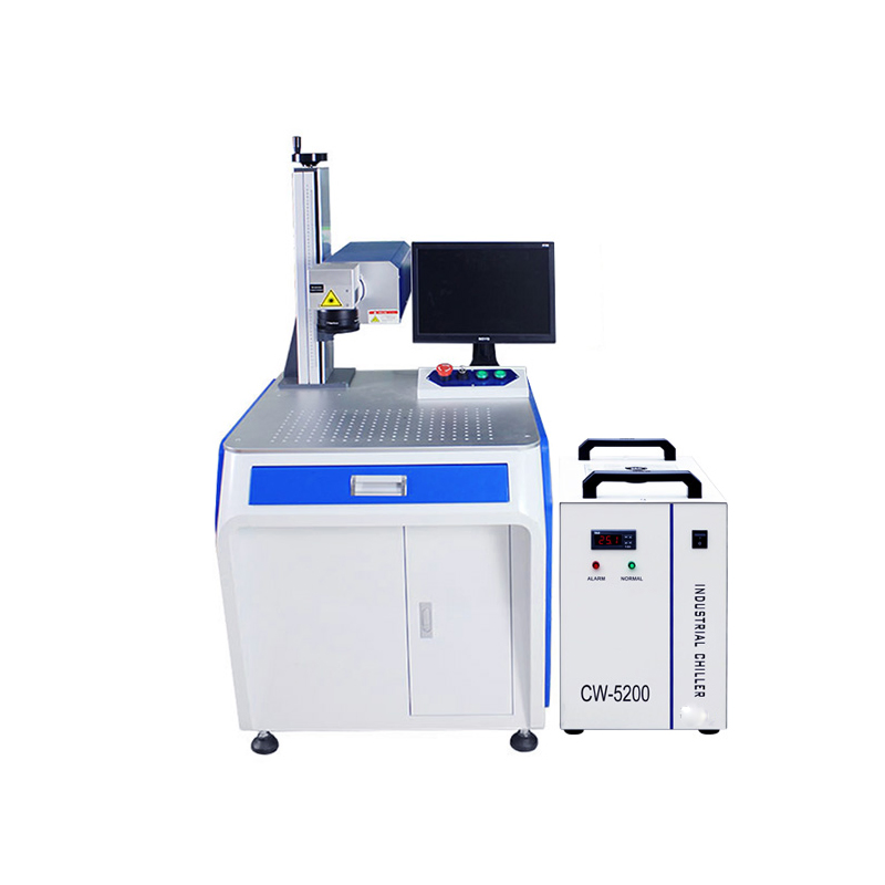
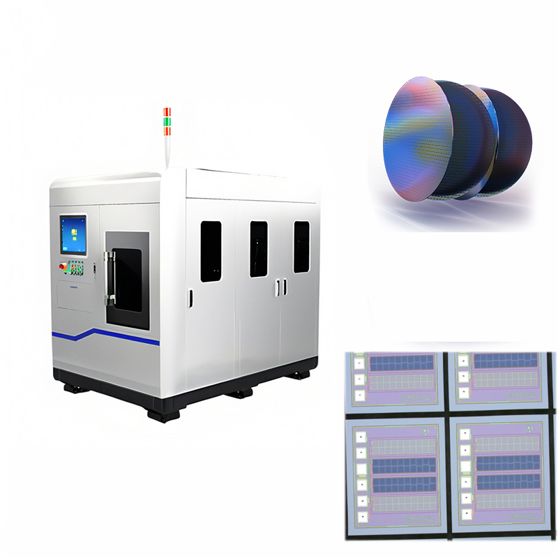
High Precision Wafer Identification and Secure Storage System
USD 50000.00 – 200000.00
/ set
Price varies by quantity and specifications
| MOQ | 1 set |
| Category | Instruments & Meters |

7
Years
98%
Response
24h
Reply
More from this Supplier
Product Description
No detailed description available. Please send an inquiry for more information.
Technical Specifications
| Model NO. | Himalaya-16 |
| After-sales Service | 12 Months |
| Function | High Temperature Resistance |
| Demoulding | Automatic |
| Condition | New |
| Certification | ISO |
| Warranty | 12 Months |
| Automatic Grade | Automatic |
| Installation | Desktop |
| Driven Type | Electric |
| Mould Life | >1,000,000 Shots |
| Leakage Rate | ≤0.5% |
| Inspection Rate | ≤3% |
| 2X Lens | Defect ≥9.7um |
| Incoming Wafer Size | 8-Inch (200mm Diameter) |
| Yield Repeatability | <±0.05% (for Non-Abnormal Wafers ≥95% |
| Wafer Detection Area | Selectable (Supports Roi) |
| Wafer Size | Adjustable |
| Foup ID | Automatic Reading, Box Opening & Mapping Scan |
| Xyz Table | Software-Controlled Interface |
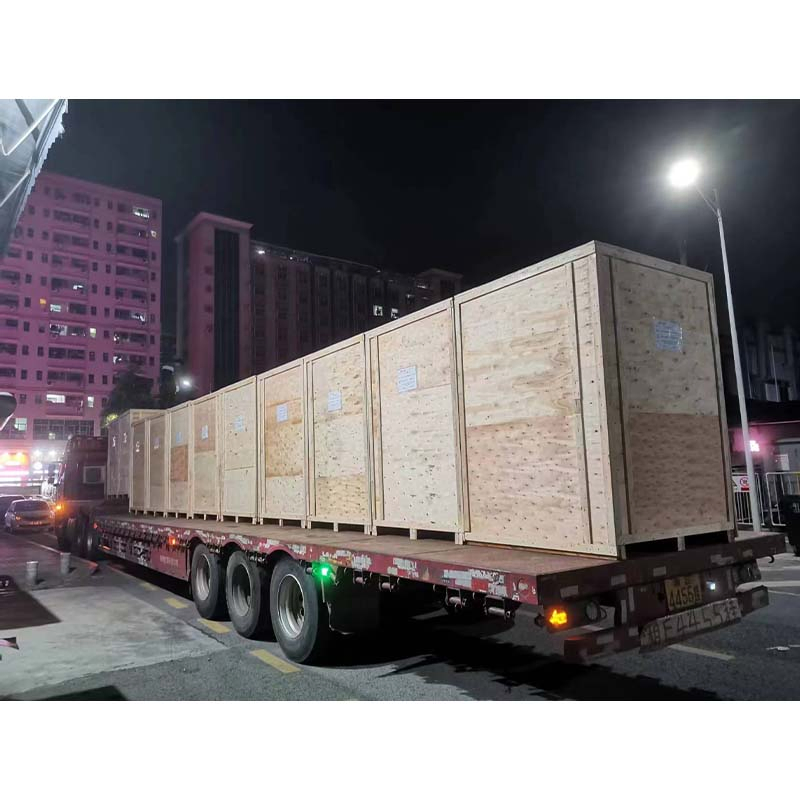
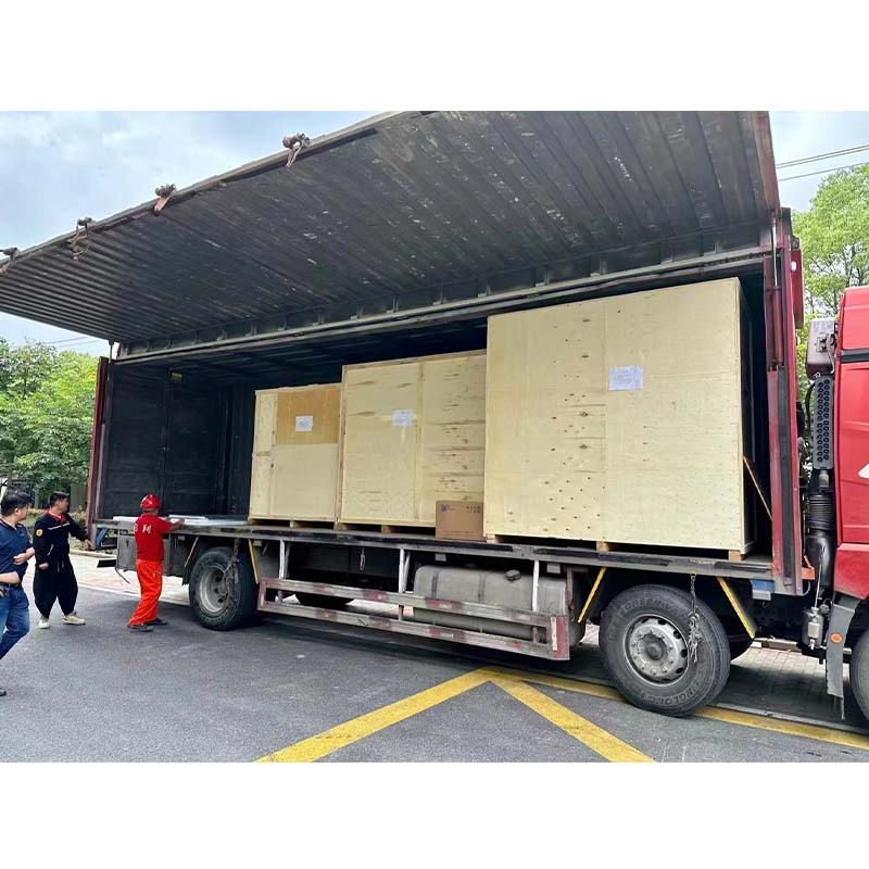
| Transport Package | Wooden Pack |
| Specification | Customized |
| Trademark | Himalaya |
| Origin | China |